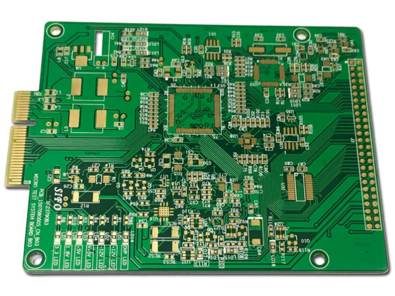
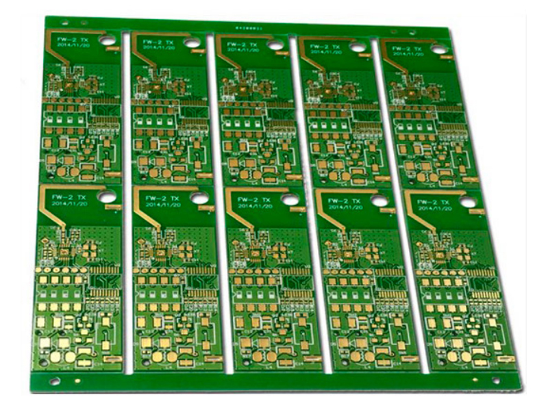
What is High-Precision PCBs
High-precision printed circuit board, also known as high-precision printed circuit board,
is an electronic component that is widely used in applications that require accurate and precise circuits.
These PCBs are designed and manufactured with great attention to detail, ensuring the highest level of accuracy and reliability.
High-precision PCBs are commonly used in industries such as aerospace, medical equipment, telecommunications, and automotive. They are especially valuable in applications requiring precise signal integrity, high frequency performance, tight tolerances, and advanced technology integration.
These PCBs are typically manufactured using advanced processes and techniques such as controlled impedance wiring, fine pitch components, micro vias, blind and buried vias, and high density interconnects. They may also involve multiple layers, complex circuits and specialized materials to meet the specific requirements of the intended application.
The manufacturing process of high-precision PCBs involves strict quality control measures, including rigorous testing and inspection procedures, to ensure that the final product meets the required specifications. This precision and accuracy enables efficient and reliable performance, especially in complex electronic systems.
CAPEL High-Precision PCBs
High-precision PCBs are designed to provide reliable and precise electrical connections. They undergo various professional manufacturing processes and adhere to strict design and testing standards to meet the specific needs of demanding applications in various industries.
High-Quality Materials
High-precision PCBs are usually made using high-quality materials, such as specialized high-speed laminates or advanced ceramics. These materials have specific properties that help improve a PCB's electrical performance and signal integrity.
Multi-Layer Structure
High-precision PCBs usually have a multi-layer structure, enabling more complex and denser circuit designs. Multi-layer construction helps improve signal isolation, reduce crosstalk and optimize power distribution.
Fine Line and Space
High-precision PCBs often require very fine line and space widths, usually measured in microns. These narrow traces allow for better signal routing and reduce signal loss or interference.
Controlled Impedance
Impedance control is critical for maintaining signal integrity in high-speed applications. A precision PCB controls the impedance of the entire trace to match the characteristic impedance required by the design.
Advanced Technology
High-precision PCBs usually use advanced manufacturing technologies such as laser drilling and direct imaging. Laser drilling enables smaller, more precise via dimensions, while direct imaging enables more accurate solder mask registration.
Testing and Inspection
Quality control is critical for high-precision PCBs. Rigorous testing and inspection processes such as automated optical inspection (AOI) and X-ray inspection are employed to identify any potential defects or issues and ensure that the PCB meets the required specifications.
Design for Manufacturability
High-precision PCBs require comprehensive DFM considerations during the design phase to ensure that designs can be manufactured efficiently and accurately. DFM techniques help optimize the design of the manufacturing process and increase overall manufacturing yield.
Miniaturized Components
High-precision PCBs are often designed to accommodate miniaturized components such as surface mount devices microelectromechanical systems (MEMS). Precise placement and soldering of these smaller components contribute to the overall accuracy and functionality of the PCB.


