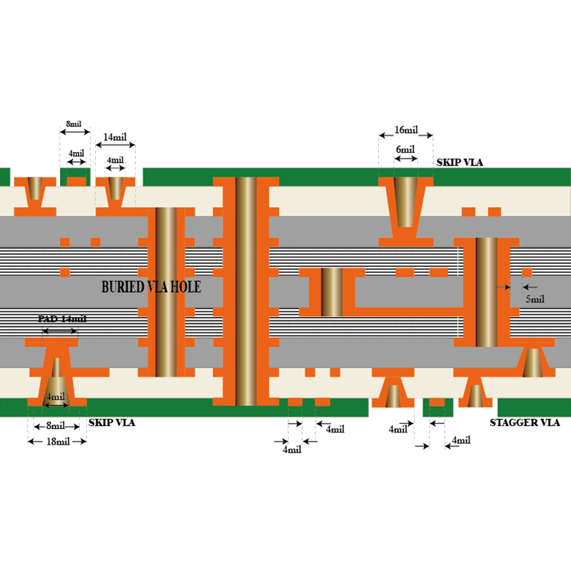
HDI PCBs (High Density Interconnect Printed Circuit Boards) have gained popularity in recent years due to their numerous advantages over conventional PCBs. As technology continues to advance and devices become smaller, faster and more complex, the demand for HDI Board continues to grow. In order to let everyone better understand HDI PCB, now Capel will explore the advantages of using HDI PCBs and how they can benefit various industries and applications in this blog .
HDI PCBs are known for their ability to accommodate high-density, complex and miniaturized circuits. Their increased number of interconnections per unit area allows for the design and integration of more features and functions in a smaller space. This is achieved by using advanced techniques such as microvias, blind and buried vias.
One of the main advantages of using HDI PCB is its enhanced electrical performance. Reduced size and shorter interconnect lengths reduce signal loss, improve signal integrity, and increase transmission speeds. This makes them ideal for high-frequency applications such as telecom, datacom, and medical equipment, where reliable and fast signal transmission is critical.
Another advantage of HDI PCB is the improved reliability and stability. High-density interconnects and the use of advanced materials such as resin-coated copper (RCC) and thin-core substrates reduce the risk of impedance mismatch, signal crosstalk and electromagnetic interference (EMI). Additionally, the elimination of through-hole components and the use of blind and buried vias enhances structural integrity and eliminates the risk of solder joint failure, making HDI PCBs more robust and durable.
In addition, HDI PCBs offer significant design flexibility. Their compact size enables the creation of smaller and lighter electronic devices, which is especially beneficial for industries such as automotive, aerospace and wearable technology. The increased interconnect count also provides greater freedom in component placement and routing, resulting in more efficient use of space and better thermal dissipation.
For manufacturers, HDI PCBs offer several advantages in terms of productivity and cost savings. The miniaturization of components and the reduction in the number of layers required can reduce material costs. The use of advanced manufacturing techniques such as laser drilling and sequential build processes simplifies the manufacturing process, shortens lead times, and minimizes the need for manual labor, increasing overall productivity.
The advantages of HDI PCB are not only reflected in the technical aspect. Their compact size and improved performance allow for the creation of sleeker, better-looking devices. This is especially important for consumer electronics, where design and appearance play an important role in consumers’ purchasing decisions.
In summary, HDI board have a wide range of advantages that make them very popular in today’s fast-paced and technology-driven world. Their high-density interconnects, improved electrical performance, enhanced reliability, design flexibility, and cost savings make them the first choice for a wide variety of industries and applications. HDI PCBs are likely to become even more popular as technology continues to advance, reshaping the way electronic devices are designed and manufactured.Shenzhen Capel Technology Co., Ltd. specializes in HDI circuit board manufacturing, utilizing our expertise and advanced facilities to provide high-quality, reliable and cost-effective solutions according to customers’ specific requirements. Whether it’s prototyping or mass production, our experienced team is dedicated to delivering best-in-class HDI PCB solutions for your projects.
Post time: Aug-23-2023
Back


