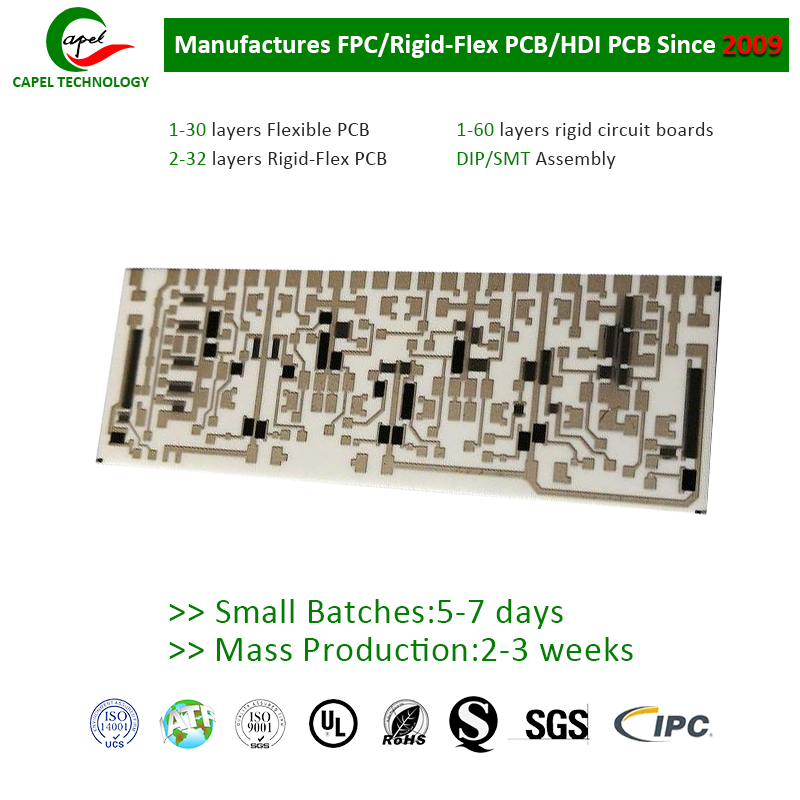
But have you ever wondered how these ceramic circuit boards are made? What steps are involved in their manufacturing process? In this blog post, we’ll take a deep dive into the complex world of ceramic circuit board manufacturing, exploring every step involved in its creation.
The world of electronics is constantly evolving, and so are the materials used to make electronic devices. Ceramic circuit boards, also known as ceramic PCBs, have gained popularity in recent years due to their excellent thermal conductivity and electrical insulation properties. These boards offer numerous advantages over traditional printed circuit boards (PCBs), making them ideal for a variety of applications where thermal dissipation and reliability are critical.
Step 1: Design and Prototype
The first step in the ceramic circuit board manufacturing process begins with the design and prototyping of the circuit board. This involves using specialized software to create a schematic and determine the layout and placement of components. Once the initial design is complete, prototypes are developed to test the board’s functionality and performance before entering the volume production phase.
Step 2: Material preparation
Once the prototype is approved, ceramic materials need to be prepared. Ceramic circuit boards are usually made of aluminum oxide (aluminum oxide) or aluminum nitride (AlN). The selected materials are ground and mixed with additives to enhance their properties, such as thermal conductivity and mechanical strength. This mixture is then pressed into sheets or green tapes, ready for further processing.
Step 3: Substrate Formation
During this step, the green tape or sheet undergoes a process called substrate formation. This involves drying the ceramic material to remove moisture and then cutting it into the desired shape and size. CNC (computer numerical control) machines or laser cutters are often used to achieve precise dimensions.
Step 4: Circuit Patterning
After the ceramic substrate is formed, the next step is circuit patterning. This is where a thin layer of conductive material, such as copper, is deposited onto the surface of the substrate using various techniques. The most common method is screen printing, where a template with the desired circuit pattern is placed on the substrate and conductive ink is forced through the template onto the surface.
Step 5: Sintering
After the circuit pattern is formed, the ceramic circuit board undergoes a critical process called sintering. Sintering involves heating the plates to high temperatures in a controlled atmosphere, usually in a kiln. This process fuses ceramic materials and conductive traces together to create a strong and durable circuit board.
Step 6: Metallization and Plating
Once the board is sintered, the next step is metallization. This involves depositing a thin layer of metal, such as nickel or gold, over the exposed copper traces. Metallization serves two purposes – it protects the copper from oxidation and provides a better solderable surface.
After metallization, the board may undergo additional plating processes. Electroplating can enhance certain properties or functions, such as providing a solderable surface finish or adding a protective coating.
Step 7: Inspect and Test
Quality control is a critical aspect of any manufacturing process, and ceramic circuit board manufacturing is no exception. After the circuit board is manufactured, it must undergo strict inspection and testing. This ensures each board meets the required specifications and standards, including checking continuity, insulation resistance and any potential defects.
Step 8: Assembly and Packaging
Once the board passes the inspection and testing stages, it is ready for assembly. Use automated equipment to solder components such as resistors, capacitors, and integrated circuits onto circuit boards. After assembly, circuit boards are typically packaged in anti-static bags or pallets, ready for shipment to their intended destination.
In summary
The ceramic circuit board manufacturing process involves several key steps, from design and prototyping to substrate formation, circuit patterning, sintering, metallization, and testing. Each step requires precision, expertise and attention to detail to ensure the final product meets the required specifications. The unique properties of ceramic circuit boards make them the first choice in a variety of industries, including aerospace, automotive and telecommunications, where reliability and thermal management are critical.
Post time: Sep-25-2023
Back


