In today’s era of rapid technological development, electronic devices have become an integral part of our daily lives. From smartphones to medical devices, printed circuit boards (PCBs) play a vital role in efficiently powering these devices. High Density Interconnect (HDI) technology PCBs have been a game changer, offering higher circuit density, improved performance and enhanced reliability. But have you ever wondered how these HDI technology PCBs are manufactured? In this article, we will dive into the intricacies of the manufacturing process and clarify the steps involved.
1. Brief introduction of HDI technology PCB:
HDI technology PCBs are popular for their ability to accommodate a large number of components in a compact design, reducing the overall size of electronic devices. These boards feature multiple layers, smaller vias, and thinner lines for greater routing density. Additionally, they offer improved electrical performance, impedance control, and signal integrity, making them ideal for high-speed and high-frequency applications.
2. Design layout:
The manufacturing journey of HDI Technology PCB starts from the design stage. Skilled engineers and designers work together to optimize circuit layout while ensuring design rules and constraints are met. Employ advanced software tools to create precise designs, defining layer stackups, component placement and routing. The layout also takes into account factors such as signal integrity, thermal management, and mechanical stability.
3. Laser drilling:
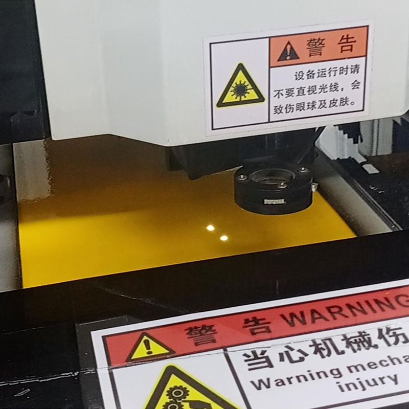
One of the key steps in HDI technology PCB manufacturing is laser drilling. Laser technology can create smaller, more precise vias, which are critical to achieving high circuit densities. Laser drilling machines use a high-energy beam of light to remove material from a substrate and create small holes. These vias are then metallized to create electrical connections between the different layers.
4. Electroless copper plating:
To ensure efficient electrical interconnection between layers, electroless copper deposition is employed. In this process, the walls of the drilled hole are coated with a very thin layer of conductive copper by chemical immersion. This copper layer acts as a seed for the subsequent electroplating process, enhancing the overall adhesion and conductivity of the copper.
5. Lamination and pressing:
HDI Technology PCB manufacturing involves multiple lamination and pressing cycles where the different layers of the circuit board are stacked and bonded together. High pressure and temperature are applied to ensure proper bonding and eliminate any air pockets or voids. The process involves the use of specialized lamination equipment to achieve the desired board thickness and mechanical stability.
6. Copper plating:
Copper plating plays a vital role in HDI technology PCBs as it establishes the necessary electrical conductivity. The process involves dipping the entire board into a copper plating solution and passing an electric current through it. Through the electroplating process, copper is deposited onto the surface of the circuit board, forming circuits, traces and surface features.
7. Surface treatment:
Surface treatment is a critical step in the manufacturing process to protect circuits and ensure long-term reliability. Common surface treatment technologies for HDI technology PCBs include immersion silver, immersion gold, organic solderability preservatives (OSP), and electroless nickel/immersion gold (ENIG). These technologies provide a protective layer that prevents oxidation, improves solderability, and eases assembly.
8. Testing and Quality Control:
Rigorous testing and quality control measures are required before HDI technology PCBs are assembled into electronic devices. Automated optical inspection (AOI) and electrical testing (E-test) are often performed to detect and correct any defects or electrical problems in the circuit. These tests ensure that the final product meets the required specifications and performs reliably.
In Conclusion:
HDI Technology PCBs have revolutionized the electronics industry, facilitating the development of smaller, lighter, and more powerful electronic devices. Understanding the complex manufacturing process behind these boards highlights the level of precision and expertise required to produce high quality HDI technology PCBs. From initial design through drilling, plating and surface preparation, every step is critical to ensure optimum performance and reliability. By employing advanced manufacturing techniques and adhering to stringent quality control standards, manufacturers can meet the ever-changing demands of the electronics market and pave the way for breakthrough innovations.
Post time: Sep-02-2023
Back


