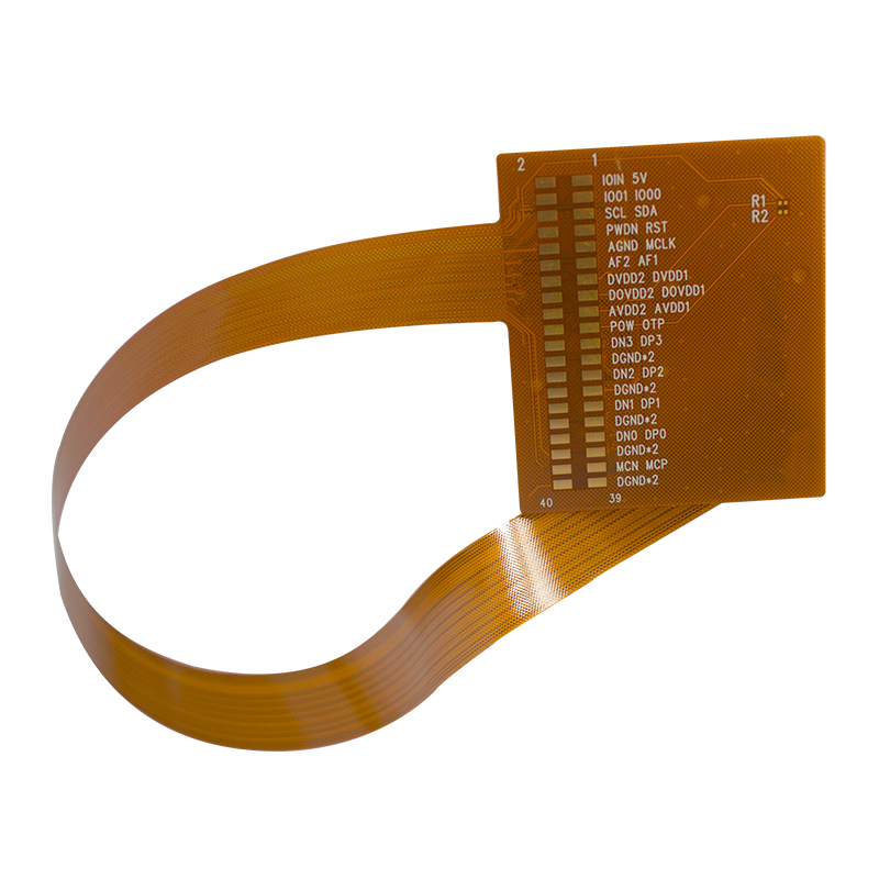
Introduce:
In today’s fast-paced world, security cameras have become an integral part of protecting our homes, businesses and public spaces. As technology advances, so does the need for innovative and more efficient security camera systems. If you are passionate about electronics and interested in security systems, you may be asking yourself: “Can I prototype a PCB for a security camera?” The answer is yes, and in this blog, we’ll walk you through a process specifically designed to Security camera PCB (printed circuit board) design and prototyping process.
Learn the basics: What is a PCB?
Before delving into the intricacies of security camera PCB prototyping, it’s important to have a basic understanding of what a PCB is. Simply put, a PCB acts as the backbone of electronic components, connecting them together mechanically and electrically to form a working circuit. It provides a compact and organized platform for components to be mounted, thereby reducing the complexity of the circuit while increasing its reliability.
Designing a PCB for Security Cameras:
1. Conceptual design:
The first step in prototyping a security camera PCB is starting with a conceptual design. Determine the specific features you want to add, such as resolution, night vision, motion detection, or PTZ (pan-tilt-zoom) functionality. Research existing security camera systems to get inspiration and ideas for your own design.
2. Scheme design:
After conceptualizing the design, the next step is to create the schematic. A schematic is a graphical representation of an electrical circuit, showing how components are interconnected. Use software tools such as Altium Designer, Eagle PCB or KiCAD to design and simulate PCB layouts. Make sure your schematic contains all necessary components such as image sensors, microcontrollers, power regulators, and connectors.
3. PCB layout design:
Once the schematic is complete, it’s time to convert it into a physical PCB layout. This stage involves placing the components on the circuit board and routing the necessary interconnections between them. When designing your PCB layout, consider factors such as signal integrity, noise reduction, and thermal management. Make sure components are strategically placed to minimize distractions and optimize functionality.
4. PCB production:
Once you are satisfied with the PCB design, it’s time to build the board. Export Gerber files containing the information needed by manufacturers to produce PCBs. Choose a reliable PCB manufacturer that can meet your design requirements and specifications. During this process, pay attention to important details such as layer stackup, copper thickness, and solder mask, as these factors can significantly affect the performance of the final product.
5. Assembly and testing:
Once you receive your fabricated PCB, it’s time to assemble the components onto the board. The process involves soldering various components such as image sensors, microcontrollers, connectors, and power regulators onto the PCB. Once assembly is complete, thoroughly test the functionality of the PCB to ensure that all components are working as expected. If any issues are detected, fix them before proceeding to the next step.
6. Firmware development:
To bring PCBs to life, firmware development is critical. Depending on the capabilities and features of your security camera, you may need to develop firmware that controls aspects such as image processing, motion detection algorithms, or video encoding. Decide on the appropriate programming language for your microcontroller and use an IDE (Integrated Development Environment) such as Arduino or MPLAB X to program the firmware.
7. System integration:
Once the firmware is successfully developed, the PCB can be integrated into a complete security camera system. This involves connecting the PCB to the necessary peripherals such as lenses, housings, IR illuminators and power supplies. Make sure all connections are tight and properly aligned. Extensive testing is performed to verify the functionality and reliability of the integrated system.
In conclusion:
Prototyping a PCB for a security camera requires a combination of technical knowledge, creativity, and attention to detail. By following the steps outlined in this blog, you can turn your ideas into reality and create a functional prototype for your security camera system. Keep in mind that the design and prototyping process may involve iteration and refinement until the desired result is achieved. With determination and perseverance, you can contribute to the ever-growing field of security camera systems. Happy prototyping!
Post time: Oct-26-2023
Back


