-
Perfect surface finish for your 14-layer FPC flexible circuit board
In this blog post, we will discuss the importance of surface treatment for 14-layer FPC flexible circuit boards and guide you in choosing the perfect treatment for your board. Circuit boards play a vital role when it comes to designing and manufacturing high-quality electronic products. If you ar...Read more -

Ensures stability and minimizes noise in 12-layer PCBs for sensitive signal, high voltage applications
Circuit boards are the backbone of any electronic device, supporting the flow of signals and power. However, when it comes to complex designs such as 12-layer boards used in sensitive signal transmission and high-voltage applications, power supply stability and noise issues can become troublesome...Read more -
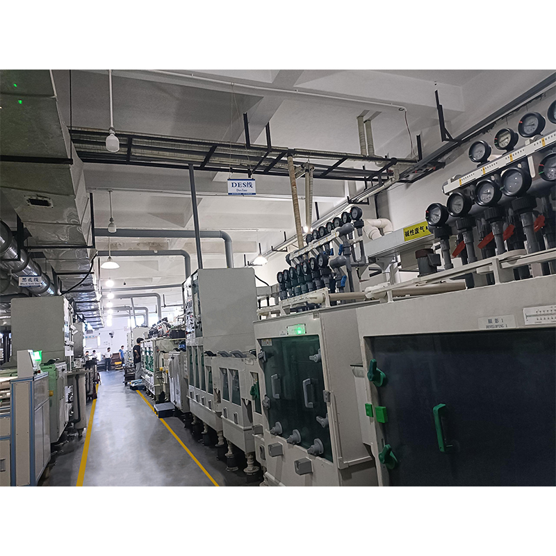
Cleaning and Anti-contamination Measures | Flexible Pcb Manufacturing | Appearance and Performance
In flexible PCB manufacturing, a key aspect that cannot be ignored is cleaning and anti-contamination measures. These measures go a long way in maintaining the appearance and performance of the circuit board. In this blog post, we will discuss how to choose the most appropriate cleaning and anti-...Read more -
Solve EMI issues in flexible PCB fabrication for high-frequency and high-speed applications
Flexible circuit fabrication is widely used in various industries due to its many advantages such as flexibility, lightweight, compactness and high reliability. However, like any other technological advancement, it comes with its fair share of challenges and drawbacks. A major challenge in flexib...Read more -
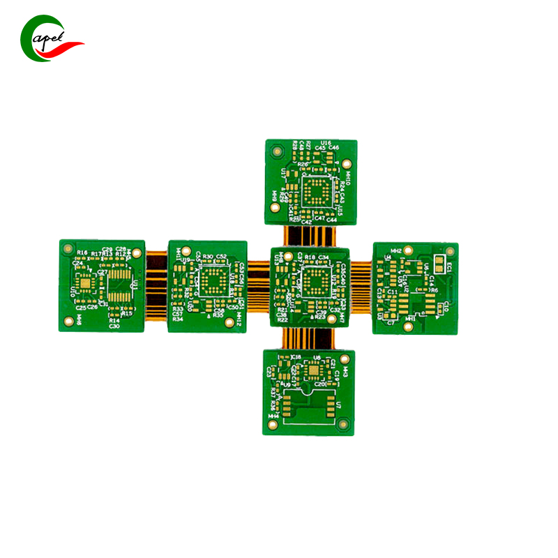
Optimize HDI Flex PCB layout and connections to improve signal quality and reduce trace length
Introduce: In this blog post, we will explore the important considerations and techniques to follow to reduce trace length and ultimately improve HDI flex PCB signal quality. High-density interconnect (HDI) flexible printed circuit boards (PCBs) are an increasingly popular choice in modern electr...Read more -
Thermal coupling and heat conduction | Rigid Flex Rigid Pcb | high-power | high-temperature environments
In today’s fast-paced technological world, the demand for electronic devices continues to grow at an astonishing rate. From smartphones to medical devices, the need for efficient and reliable circuit boards is critical. One particular type of circuit board that is becoming more and more pop...Read more -

Optimize signal quality in 12-layer PCBs to reduce crosstalk
Solving Routing and Interlayer Connection Challenges in 12-Layer Circuit Boards to Achieve Optimal Signal Quality and Reduce Crosstalk Introduce: Rapid advances in technology have led to an increase in the demand for complex electronic devices, resulting in the use of multi-layer circuit boards. ...Read more -
Vibration-damping materials in the 14-layer flexible PCB were selected to protect against mechanical shock
How to choose damping and vibration reduction materials suitable for 14-layer flex pcb to prevent the impact of mechanical vibration and impact on the circuit board? Introduce: As technology advances and electronic devices continue to shrink in size, the importance of vibration and shock protecti...Read more -

Stack-up and inter-layer connectivity in 10-layer circuit boards
Introduce: This blog aims to explore effective strategies for solving 10-layer circuit board stacking and inter-layer connection issues, ultimately enhancing signal transmission and integrity. In the ever-evolving world of electronics, circuit boards play a vital role in connecting various compon...Read more -

Solve 8 Layer Pcb signal integrity and clock distribution problems
If you’re involved in electronics and printed circuit boards (PCBs), you’ve probably encountered common challenges with signal integrity and clock distribution. These issues can be difficult to overcome, but have no fear! In this blog post, we will explore how to solve signal integrit...Read more -

6 Layer Pcb power supply stability and power supply noise problems
As technology continues to advance and equipment becomes more complex, ensuring a stable power supply becomes increasingly important. This is especially true for 6-layer PCBs, where power stability and noise issues can severely impact sensitive signal transmission and high-voltage applications. I...Read more -

Solve double sided pcb thermal expansion and thermal stress problems
Are you facing thermal expansion and thermal stress issues with double-sided PCBs? Look no further, in this blog post we will guide you on how to solve these problems effectively. But before we dive into the solutions, let’s introduce ourselves. Capel is an experienced manufacturer in the circuit...Read more


