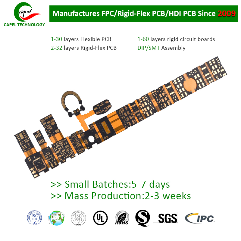
In this blog post, we will explore various techniques and strategies to achieve optimal insulation performance in multi-layer PCBs.
Multilayer PCBs are widely used in various electronic devices due to their high density and compact design. However, a key aspect of designing and manufacturing these complex circuit boards is ensuring that their interlayer insulation properties meet the necessary requirements.
Insulation is crucial in multilayer PCBs as it prevents signal interference and ensures the proper functioning of the circuit. Poor insulation between layers can lead to signal leakage, crosstalk, and ultimately electronic device failure. Therefore, it is critical to consider and implement the following measures during the design and manufacturing process:
1. Choose the right material:
The choice of materials used in a multilayer PCB structure greatly affects its interlayer insulation properties. Insulating materials such as prepreg and core materials should have high breakdown voltage, low dielectric constant and low dissipation factor. Additionally, considering materials with good moisture resistance and thermal stability is critical to maintaining insulation properties over the long term.
2. Controllable impedance design:
Proper control of impedance levels in multilayer PCB designs is critical to ensuring optimal signal integrity and avoiding signal distortion. By carefully calculating trace widths, spacing, and layer thicknesses, the risk of signal leakage due to improper insulation can be significantly reduced. Achieve accurate and consistent impedance values with the impedance calculator and design rules provided by PCB manufacturing software.
3. The insulation layer thickness is sufficient:
The thickness of the insulation layer between adjacent copper layers plays a vital role in preventing leakage and enhancing overall insulation performance. Design guidelines recommend maintaining a minimum insulation thickness to prevent electrical breakdown. It is critical to balance thickness to meet insulation requirements without negatively affecting the overall thickness and flexibility of the PCB.
4. Proper alignment and registration:
During lamination, correct alignment and registration between the core and prepreg layers must be ensured. Misalignment or registration errors can lead to uneven air gaps or insulation thickness, ultimately affecting interlayer insulation performance. Utilizing advanced automated optical alignment systems can significantly improve the accuracy and consistency of your lamination process.
5. Controlled lamination process:
The lamination process is a key step in multi-layer PCB manufacturing, which directly affects the interlayer insulation performance. Strict process control parameters such as pressure, temperature and time should be implemented to achieve uniform and reliable insulation across layers. Regular monitoring and verification of the lamination process ensures consistency of insulation quality throughout the production process.
6. Inspection and testing:
To ensure that the interlayer insulation performance of multi-layer PCBs meets the required standards, strict inspection and testing procedures should be implemented. Insulation performance is typically evaluated using high voltage testing, insulation resistance measurements, and thermal cycle testing. Any defective boards or layers should be identified and corrected before further processing or shipment.
By focusing on these critical aspects, designers and manufacturers can ensure that the interlayer insulation performance of multilayer PCBs meets the necessary requirements. Investing time and resources into proper material selection, controlled impedance design, adequate insulation thickness, precise alignment, controlled lamination, and rigorous testing will result in a reliable, high-performance multilayer PCB.
In summary
Achieving optimal interlayer insulation performance is critical for reliable operation of multilayer PCBs in electronic devices. Implementing the techniques and strategies discussed during the design and manufacturing process will help minimize signal interference, crosstalk, and potential failures. Remember, proper insulation is the foundation of efficient, robust PCB design.
Post time: Sep-26-2023
Back


