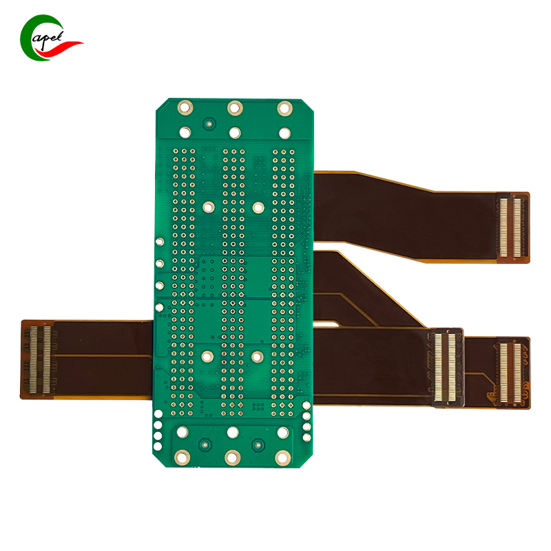
Prototyping a printed circuit board (PCB) with low noise requirements can be a challenging task, but it is definitely achievable with the right approach and understanding of the principles and techniques involved. In this blog post, we’ll explore the steps and considerations that can help you create low-noise PCB prototypes. So, let’s get started!
1. Understand noise in PCBs
Before delving into the prototyping process, it is necessary to understand what noise is and how it affects PCBs. In PCB, noise refers to unwanted electrical signals that can cause interference and disrupt the desired signal path. Noise can be caused by a variety of factors, including electromagnetic interference (EMI), ground loops, and improper component placement.
2. Select noise optimization components
Component selection is critical to minimizing noise in PCB prototypes. Choose components specifically designed to reduce noise emissions, such as low-noise amplifiers and filters. Additionally, consider using surface mount devices (SMDs) instead of through-hole components, as they can reduce parasitic capacitance and inductance, thus providing better noise performance.
3. Correct component placement and routing
Careful planning of the placement of components on a PCB can significantly reduce noise. Group noise-sensitive components together and away from high-power or high-frequency components. This helps minimize the risk of noise coupling between different circuit parts. When routing, try to separate high-speed signals and low-speed signals to prevent unnecessary signal interference.
4. Ground and power layers
Proper grounding and power distribution are critical to noise-free PCB design. Use dedicated ground and power planes to provide low-impedance return paths for high-frequency currents. This helps reduce voltage fluctuations and ensures a stable signal reference, minimizing noise in the process. Separating analog and digital signal grounds further reduces the risk of noise contamination.
5. Noise reduction circuit technology
Implementing noise reduction circuit techniques can help improve the overall noise performance of PCB prototypes. For example, using decoupling capacitors on the power rails and close to active components can suppress high-frequency noise. Utilizing shielding techniques, such as placing critical circuitry in metal enclosures or adding grounded shielding, can also minimize EMI-related noise.
6. Simulation and testing
Before a PCB prototype is manufactured, its performance must be simulated and tested to identify and resolve any potential noise-related issues. Use simulation tools to analyze signal integrity, account for parasitic components, and evaluate noise propagation. Additionally, functional testing is performed to ensure the PCB meets the required low-noise requirements before proceeding with production.
In summary
Prototyping PCBs with low noise requirements requires careful planning and implementation of various techniques. You can significantly reduce noise in your PCB design by selecting noise-optimized components, paying attention to component placement and routing, optimizing ground and power planes, utilizing noise-reducing circuit techniques, and thoroughly testing prototypes.
Post time: Oct-29-2023
Back


