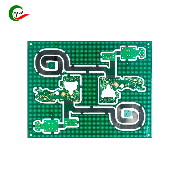
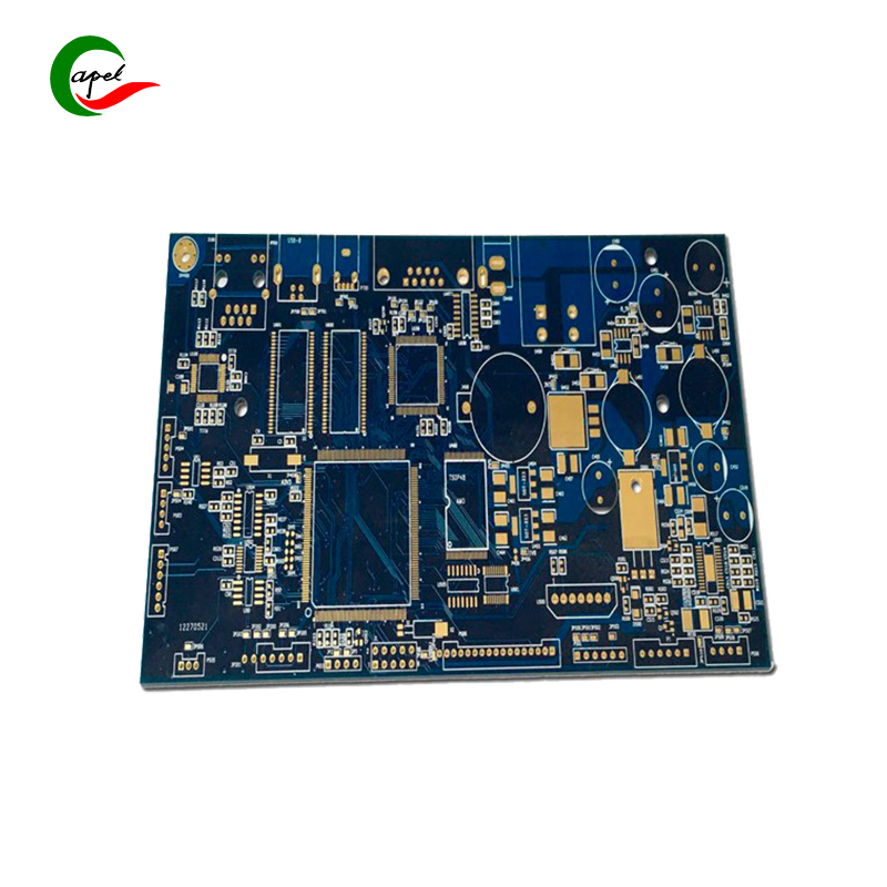
Understand the key differences between HDI PCB and traditional Circuit Board:
Printed circuit boards (PCBs) are an important component in the manufacture of electronic equipment. They serve as a base, connecting various electronic components to create functional devices. Over the years, PCB technology has advanced significantly, and high-density interconnect (HDI) boards have become more and more popular. In this blog post, we’ll explore the key differences between HDI and traditional PCBs, clarifying their unique characteristics and advantages.
1. Design Complexity
Conventional PCBs are usually designed in single-layer or double-layer configurations. These boards are often used in simple electronic devices where space constraints are minimal. HDI PCBs, on the other hand, are much more complex to design. They consist of multiple layers with complex patterns and interconnected circuits. HDI boards are best suited for compact devices with limited space and high performance requirements, such as smartphones, tablets, and wearable technology.
2. Component density
One of the main differences between HDI and traditional PCB is its component density. HDI boards offer higher component density, enabling smaller and lighter devices. They do this by utilizing microvias, blind and buried vias. Microvias are small holes in a PCB that interconnect different layers, allowing the efficient flow of electrical signals. Blind and buried vias, as the name suggests, extend only partially or are completely hidden within the board, further increasing its density. Although reliable, traditional PCBs cannot match the component density of HDI boards and are more suitable for low-density applications.
3. Signal integrity and performance
As technology continues to advance, the need for high-speed and high-performance devices continues to increase. HDI PCBs are specifically designed to meet these needs. Shorter electrical paths in HDI boards reduce transmission line effects such as signal loss and electromagnetic interference, thereby improving signal integrity. Additionally, the reduced size of the HDI board enables more efficient signal propagation and faster data transfer. Traditional PCBs, while reliable, may struggle to maintain the same level of signal integrity and performance as HDI boards.
4. Manufacturing process
The manufacturing process of HDI PCB is different from traditional PCB. HDI boards require advanced manufacturing techniques such as laser drilling and sequential lamination. Laser drilling is used to create microscopic holes and precise patterns on the surface of the circuit board. Sequential lamination is the process of layering and bonding multilayer PCBs together to form a dense and compact structure. These manufacturing processes result in a higher cost for HDI boards compared to conventional PCBs. However, the benefits of improved performance and smaller form factors often outweigh the additional cost.
5. Design flexibility
Compared with traditional PCBs, HDI PCBs provide greater design flexibility. Multiple layers and compact size allow for more creative and intricate designs. HDI technology enables designers to address demands for innovative product features such as densely packed components and reduced overall size. Traditional PCBs are reliable but have limited design flexibility. They are better suited for simple applications without strict size constraints.
In summary, HDI pcb and Traditional Circuit Board are designed to meet different requirements and specifications. HDI boards are best suited for high-density applications with demanding performance criteria, while traditional PCBs are a cost-effective solution for low-density applications. Knowing the key differences between these two types of PCBs is critical to choosing the right option for your electronic device. As technology continues to evolve, HDI boards are likely to become more common in the industry, driving innovation and pushing the boundaries of electronic design.
Post time: Aug-20-2023
Back


